


SiC Wafer Manufacturers and Suppliers
SiC Wafer Manufacturers and Suppliers
Negotiable Min Order Quantity Unit
- Required Quantity
-
- Place of Origin
- China
- Payment Terms
- T/T
- Production method
- Available
- Shipping / Lead Time
- Negotiable / Negotiable
- Category
- Semiconductors
![]()
Suzhou Hengmairui Materials Technology Co.,Ltd.
 China
China
- Verified Certificate
-
10


| Product name | SiC Wafer Manufacturers and Suppliers | Certification | - |
|---|---|---|---|
| Category | Semiconductors | Material | - |
| Keyword | sic wafer manufacturers , sic substrate manufacturers | Unit Size | - |
| Brand name | - | Unit Weigh | - |
| origin | China | Stock | 25 |
| Supply type | Available | HS code | - |
Product Information
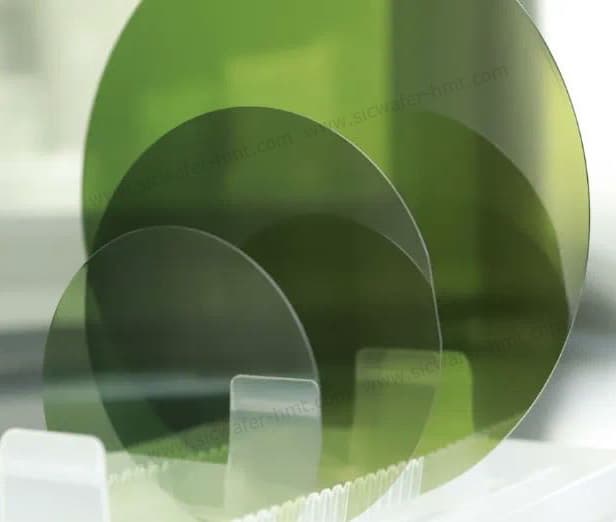
SiC Wafer Manufacturer HMT provide 2 inch to 8 inch on axis and off axis SiC wafer with 4H polytype. Normally Conductive N type SiC Wafer orientation is off axis 4.0 toward<1120>±0.5° and Semi-insulated SI type SiC wafer orientation is on axis <0001>±0.25°. We supply all grades of SiC Wafer based on different customers requirements. Meanwhile, we also offer all diameters (2 inch 4 inch 6 inch and 8inch) As cut SiC wafers without lapping and polishing and SiC Boules.
The output of a single 8-inch SiC substrate chip is about 2 times that of a 6-inch, 4 times that of a 4-inch, and can be partially equipped with silicon-based power chip production lines, which can greatly reduce costs and improve efficiency.
Taking the 32mm² area of bare metal (chip) as an example, the number of bare metal on the 8-inch SiC substrate increased by nearly 90% compared to the 6-inch, while the proportion of the edge bare metal was reduced from 14% to 7%, and the utilization rate of the 8-inch substrate increased by 7% compared to the 6-inch.
B2B Trade
| Price (FOB) | Negotiable | transportation | Express |
|---|---|---|---|
| MOQ | Negotiable | Leadtime | Negotiable |
| Payment Options | T/T | Shipping time | Negotiable |
![]()
- President
- Cory
- Address
- LiSheng Industrial Building,60 Suli Road
- Product Category
- Semiconductors
- Year Established
- 2009
- No. of Total Employees
- 51-100
- Company introduction
-
Homray Material Technology(HMT)was established in 2009, is a leading manufacturer and supplier of Gallium Nitride(GaN) Substrate Wafer(GaN-On-Sapphire Template, Free-standing GaN Wafer), GaN Epi Wafer (GaN-On-Si Epi Wafer, GaN-On-Sapphire Epi Wafer, GaN-On-SiC Epi Wafer), and Silicon Carbide(SiC) Substrate Wafer, SiC Epi Wafer, Silicon Test Wafer etc. It is widely acknowledged that compound Semiconductor (GaN, SiC) with its superior property like wide-bandgap, is expected to the most promising material choice for next generation device. GaN device/module and SiC device/module can achieve low losses and fast switching/oscillation simultaneously because of its high critical electrical field. Homray Material Technology is committed to developing high quality GaN Wafer and SiC Wafer for HEMT RF, power electronics and opto-electronics applications. As the leading Substrate Wafer and Epi Wafer manufacturer and supplier in the semiconductor industry, our dealers and partners are mainly distributed in Europe, USA, Southeast Asia, and South America, our sales value exceeded 65 Million US dollars in 2020. Excellent products quality and professional service won the trust and support from our customers in the world as well as our share of market.
- Main Product


 Lead Frame Magazine with wire stopper.jpg "Plazma (Perforated) Lead Frame Magazine with wire stopper")


