


P type test silicon wafer supplier si substrate
Negotiable Min Order Quantity Unit
- Required Quantity
-
- Place of Origin
- China
- Payment Terms
- T/T
- Production method
- Negotiable
- Shipping / Lead Time
- Negotiable / Negotiable
- Keyword
- silicon wafer supplier, si substrate
- Category
- Semiconductors
Apply a video call to the Supplier
![]()
Suzhou Hengmairui Materials Technology Co.,Ltd.
- Membership
- BIZ
- Recent Visit
- Jun 28, 2024
- Country / Year Established
-
 China
/
2009
China
/
2009
- Business type
- Manufacturer
- Verified Certificate
-
9


| Product name | P type test silicon wafer supplier si substrate | Certification | - |
|---|---|---|---|
| Category | Semiconductors | Ingredients | - |
| Keyword | silicon wafer supplier , si substrate | Unit Size | - |
| Brand name | - | Unit Weigh | - |
| origin | China | Stock | - |
| Supply type | - | HS code | - |
Product Information
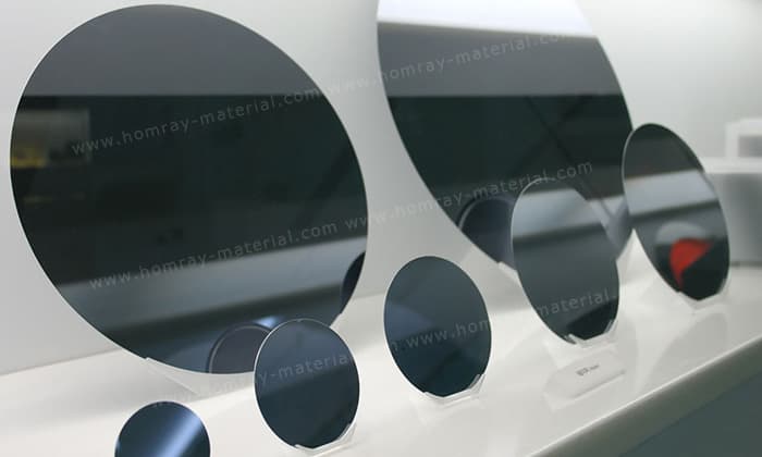
test silicon wafer,silicon test wafer supplier
Test Grade Wafers are high quality wafers which have less comprehensive specifications than a prime grade wafer.
These wafers monitor the performance and conditions of a particular semiconductor processing step. The Test Grade Wafer provides a more economical solution for isolated testing.
Place of Origin: China (Mainland)
Brand Name: Homray Material Technology
Orientation:100 111 110
Grade:Production Grade/Research Grade/Dummy Grade
Keyword: Polished silicon wafer
Type: N/P
Size: 3/4/5/6/8/12
Resistivity: 0.001-10000 Ω.cm
Surface: Polished
Application: semiconductor
B2B Trade
| Price (FOB) | Negotiable | transportation | - |
|---|---|---|---|
| MOQ | Negotiable | Leadtime | Negotiable |
| Payment Options | T/T | Shipping time | Negotiable |
![]()
- President
- Cory
- Address
- LiSheng Industrial Building,60 Suli Road
- Product Category
- Semiconductors
- Year Established
- 2009
- No. of Total Employees
- 51-100
- Company introduction
-
Homray Material Technology(HMT)was established in 2009, is a leading manufacturer and supplier of Gallium Nitride(GaN) Substrate Wafer(GaN-On-Sapphire Template, Free-standing GaN Wafer), GaN Epi Wafer (GaN-On-Si Epi Wafer, GaN-On-Sapphire Epi Wafer, GaN-On-SiC Epi Wafer), and Silicon Carbide(SiC) Substrate Wafer, SiC Epi Wafer, Silicon Test Wafer etc. It is widely acknowledged that compound Semiconductor (GaN, SiC) with its superior property like wide-bandgap, is expected to the most promising material choice for next generation device. GaN device/module and SiC device/module can achieve low losses and fast switching/oscillation simultaneously because of its high critical electrical field. Homray Material Technology is committed to developing high quality GaN Wafer and SiC Wafer for HEMT RF, power electronics and opto-electronics applications. As the leading Substrate Wafer and Epi Wafer manufacturer and supplier in the semiconductor industry, our dealers and partners are mainly distributed in Europe, USA, Southeast Asia, and South America, our sales value exceeded 65 Million US dollars in 2020. Excellent products quality and professional service won the trust and support from our customers in the world as well as our share of market.
- Main Product


_chip-set_with_DNN_Engine_2.jpg "Stand_alone TTS _Text to Speech_ chip_set with DNN Engine_1")

_2.jpg "MFC _Mass Flow Controller__1")
