Image Sensor Chip -NeoPAC
Negotiable Min Order Quantity Unit
- Required Quantity
-
- Place of Origin
- Payment Terms
- Negotiable
- Production method
- Negotiable
- Shipping / Lead Time
- Negotiable / Negotiable
- Keyword
- Category
- Digital Cameras

OPTOPAC Inc
- Verified Certificate
-
16


| Product name | Image Sensor Chip -NeoPAC | Certification | - |
|---|---|---|---|
| Category | Digital Cameras | Ingredients | - |
| Keyword | - | Unit Size | - |
| Brand name | - | Unit Weigh | - |
| origin | Stock | - | |
| Supply type | - | HS code | - |
Product Information
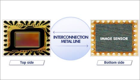
NeoPAC® is the name of our patented image sensor chip scale package
Conventional camera module has been used COB(Chip on board) structure which is connecting electrical signals between sensor die pads and PCB pads by using gold bonding wire.
NeoPAC is a new style of package structure which is using solder joint between electro copper plated glass substrate and lead free solder bumped sensor dies. Meanwhile, electrical connection between the package and PCB made through outer solder balls on the glass substrate


NeoPAC® Advantages
- Low cost, high volume producible chip scale package solution which using proven semiconductor technology and equipments.
- High cum yield by assembling good sensor die and good glass window.
- High reliability image sensor SCP fulfills JEDEC MSL1
- Slim and smaller size compared to previous conventional package solutions.
- Capability of optical filter coating at the top and bottom side of glass substrate slim module solution
- Accurate co-planarity between sensor image surface and glass top surface ±5um control, easier to control image uniformity in camera module.
- Lowest clearance tolerance between image surface and glass top ±8um
- Low image plane height after SMT 0.14~0.16mm, slim module application
- Provides full image test after package together with electrical test by using automatic tester
B2B Trade
| Price (FOB) | Negotiable | transportation | - |
|---|---|---|---|
| MOQ | Negotiable | Leadtime | Negotiable |
| Payment Options | Negotiable | Shipping time | Negotiable |

- President
- DEOK-HOON KIM
- Address
- 1112-11, Namchon-ri, Oksan-myeon, Cheongwon-gun, Chungcheongbuk-do, 363-911, KOREA
- Product Category
- Electrical Equipment
- Year Established
- 2003
- No. of Total Employees
- 1-50
- Company introduction
-
OptoPAC Inc that design and develop WLCSP(Wafer Level Chip Scale Package) for CMOS and CCD Image Sensor has been grown as a venture company since Oct 2003. Also OptoPAC is based on the specific patent technologies and know-how in Image Sensor Package fields. We were the first to actualize WLCSP made use of 8" glass wafer based on the specific patent technologies. Finally, we provide our customers with the maximum satisfaction with competitive WLCSP through the price, size and reliability.
Recently, as market of Image Sensor, Camera module is advanced very rapidly, we become competitive with each other for the top of technology and quality within rapid distribution of Camera Phone and Digital Camera over the world. Under this circumstances, we will do our best for providing our customers with reliable products and services as the leader of WLCSP fields based on key technology and research.
Once again I cordially thank you for your visits to the homepage. I would like to ask you a favor that you will utilize our homepage plentifully, also you will continuously cooperate for the homepage.
- Main Markets
-
 Hong Kong(China)
 U.S.A
U.S.A
- Main Product
Related Products
EZ-CAM (EZ-300)
EZ-CAM(EZ-500/EZ-500TTS)
car dvr gps 2.7inch LCD ambarella a7 car dvr
CAMERA STRAP
Camera, custom camera, camera mould, plastic molding, camera


 South Korea


